| |
| |
Basic Study of Advanced Materials |
 |
|
|
| |
Atomic level characterization and elucidation of material’s
structures and electronic properties |
|
| |
The ultimate miniaturization of electronic devices requires that we
characterize electronic materials at the sale of atoms and analyze various
quantum effects of electrons, in order to understand and optimize functions
of nanoelectronics devices. Our research focuses on observing atomic structures
of material surfaces using scanning tunneling microscopy (STM), measuring
surface characteristics on an atomic level, and elucidating local electronic
properties of materials in order to gain further insight on their functions
in nanoelectronics.
We are also interested in atom-sized contacts and wires of metals, which
have many unique electronic and mechanical properties, not seen in macroscopic
contacts. A simple breaking-junction technique allows us to study single-atom
contacts of various metals and alloys, foreseeing their potential application
as interconnect in nanoelectronics. |
|
| |
|
|
| |
Academic staff |
|
| |
| |
|
|
| |
 |
| Professor : Sakai, Akira |
| |
| Research Topics |
| 1. |
Physics of atom-sized contacts |
| 2. |
SPM study of atomic and electronic
structures of materials |
| 3. |
Study of field emitters |
|
| |
| Contact / Office |
Room 226, School of Engineering Science
Bldg, Yoshida Campus
TEL +81-75-753-4833 • 9176
FAX +81-75-753-4841 • 9145
sakai.akira.4z kyoto-u.ac.jp kyoto-u.ac.jp |
|
| |
|
|
|
|
| |
|
|
| |
| |
|
|
| |
 |
| Associate Professor : Kurokawa, Shu |
| |
| Research Topics |
| 1. |
High spatial resolution imaging
of surface potential by scanning tunneling microscopy
(STM) |
| 2. |
Observation and control of
dopant atoms in semiconductors using STM |
| 3. |
Study of the stability of atom-sized contacts |
|
| |
| Contact / Office |
Room 224, School of Engineering Science
Bldg, Yoshida Campus
TEL +81-75-753-4832 / FAX +81-75-753-4841
kurokawa.shu.4mkyoto-u.ac.jp |
|
| |
|
|
|
|
| |
|
|
| |
|
|
| |
 |
| |
|
|
| |
|
|
| |
|
|
| |
|
|
| |
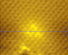
Atomic scale characterization of materials using scanning probe microscopy
(SPM) |
|
| |
Spatial fluctuations in electrostatic potential in semiconductors,
caused by ionic adsorbates and dopant atoms, are considered to make significant
influence on the performance of nano-scale devices, and their characterization
is thus a matter of primary importance. We are carrying out atomic-level
observation of the local electrostatic potential utilizing the “STM
barrier-height (STM-BH) imaging”, which combines the ultimate spatial
resolution of STM and its capability of probing local tunneling barrier
height. Since the barrier-height is related to the local surface potential,
we can obtain, with STM-BH, high-resolution mapping of electrostatic potential,
and perform pinpoint potential measurements around individual charged
adsorbates and dopants. We also develop Scanning Tunneling Potentiometry
(STP) and observe local electronic conductivity in thin films and (metal-semiconductor
and semiconductor-semiconductor) heterojunctions, in order to visualize
electronic current paths in nm resolution. |
|
| |
|
|
| |
|
|
| |
|
|
| |
|
|
| |
|
|
| |
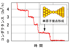
Atom-sized contacts of metals and alloys |
|
| |
A single-atom contact of metals, consisting of one atom bridging between
electrodes, is the smallest of all contacts but exhibits a variety of
interesting properties. Single-atom contacts of noble metals, for example,
have a tensile strength comparable to that of ideal crystals and show
a ballistic electron transport, leading to a universal conductance which
nicely agrees with the conductance quantum 2e2/h
(e and h are elementary charge and Planck constant, respectively). We
are studying single-atom contacts of noble metals and alloys under high-bias/high-current
conditions, employing various breaking junction techniques for forming
them. Our aim is to elucidate how much current they can sustain, how they
can be destabilized by bias/current-induced effects, and how they differ
depending on their chemical species and alloy compositions. Answering
these questions is not only important for potential applications of single-atom
contacts as interconnects in atomic and molecular electronics but also
quite interesting in it own right. |
|
| |
|
|
| |
|
|
| |
|
| |
|
|
|
|
|